This is Part 2 of a series. Part 1 can be found here, and Part 3 will be posted tomorrow.
CPUs Continued:

The Matrix Engine
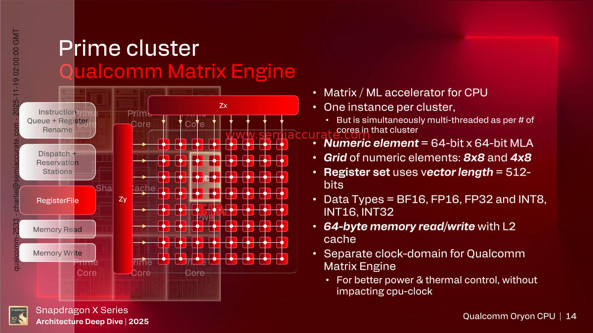
Now on to the most unique feature, the Matrix Engine, MX in the cluster slide near the top of the section. There is one MX per cluster and it is shared in a round robin fashion. The interesting thing here is that unlike many modern tack-on accelerators, this one is not seen by the cores as external. The cores have instructions that run on the MX and they are just executed as normal instructions, not bundled and sent off via DMA. To the cores, and therefor users and software, the capabilities of the MX are just part of the core, nothing special.
The MX runs on it’s own clock, said to be close to but lower than the cores, and has it’s own controller, instruction queues, registers, rename stations, dispatch, and memory access hardware. In short it is a full multi-threaded CPU with a very narrow set of instructions, all of which are fed to it by other cores. It can access the L2 directly in 64B chunks, note the capital, so it can feed the 512b vectors it uses in 1 cycle.
We asked Qualcomm about how it works, does it schedule a slot for each core in the cluster and just churn through them or is it more dynamic? The reason for this is that some companies in the past have done some rather sub-optimal scheduling in cases like this. The short answer is that Qualcomm did right and there are no bubbles or other silliness if a core does not use the MX, it just schedules another instruction instead.
Last up on the cores we have security, not to be confused with the SoC level Guardian stuff to be discussed later. In this case the Snapdragon X2 Elite line uses the full suite of ARM security technologies like Trustzone, has crypto extensions, control flow integrity, and speculation barriers. On top of that they built in preemptive side channel attack mitigation, mainly encrypting predictive structures so a non-encrypted tweak won’t result in a breach. Memory is also tagged, a good thing in almost every way. In short security isn’t an afterthought on the cores but nothing in this realm is absolute, a truism that applies to every vendor.

The Performance Cluster looks familiar
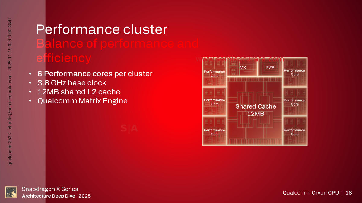
That brings us to the Performance cluster, the ‘smaller’ core of the set, but not a ‘small’ core. Again, think Mama Bear. From a high level it looks very similar to the Prime cores other than a clock of 3.6GHz base clock and a 12MB L2 cache. Qualcomm was quite reticent to disclose anything about the cores other than that they were more efficient but still quite performant. There are fewer pipes and things are optimized for lower power at the physical design stage.
With a little prodding we got the usual bits about narrower internal structures, smaller caches and buffers, and all the usual bits you would expect. When asked if it was just a re-layout of the Prime core ala AMD’s small cores or the early Apple Big/Little devices, they said it was not. Pipelines are obviously shorter because of the lower clock but the last bit was unexpected. There are some instructions that are not in the Performance cores, think internal micro-ops, nothing ISA visible. Let me repeat that, the ISA is the same between the cores, exactly.
Some instructions that may do things a bit faster than others but with a lower perf/watt ratio, they were not added to this core. To use an example that is obviously not the case here but is a good illustration, think a MAC (Multiply-Accumulate) or a MAD (Multiply-Add). If you do things in one instruction vs two, it works faster, but a dedicated multiply and add unit take up more die area and could burn more power. The things Qualcomm took out of the Performance cores are like that, you issue a MAC and it does the work but in two chunks while saving power. Users will never see anything amiss but it does shift the perf/watt curve to be more efficient.
GPU:
One of the funniest moments of the entire Qualcomm X2 brief came when the GPU speaker, Eric Demers, praised the CPU team for their ‘up to 39%’ higher performance. Right after he pointed out they got 2.3x higher performance on the GPU. You could almost sense a friendly rivalry between their teams, long may it continue. In public please.

Mobile GPUs are getting complex
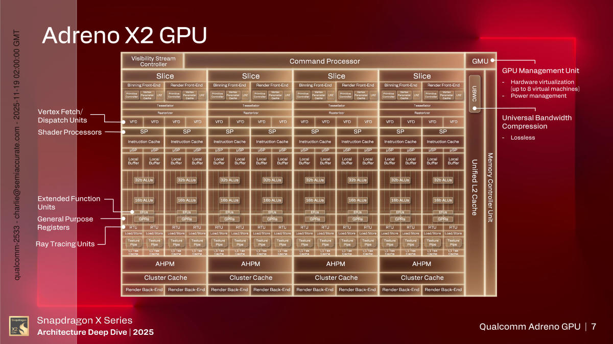
Back to the hardware some of the earlier messaging from Qualcomm has been fleshed out, the slice based architecture. As you can see above, the Adreno X2 GPU is a four slice design but externally it looks like a single unit, mobile is said to max out at three slices. There is a single command processor at the front which feeds the four slices. For performance there is 21MB of high performance memory, AHPM in the diagram, physically partitioned into 5.25MB per slice, but it is seen by all slices as a single unified cache. In short it may be sliced but unless you are deeper down in the weeds than anyone should be, it looks like one big GPU and cache.
In the top corner we have the GMU or GMU’s Mot Unix, either that or GPU Management Unit, a little historical bad humor for you there. This is a little RISC CPU that basically manages the GPU plumbing. It runs a realtime OS, controls hardware virtualization, up to eight VMs allowed, and monitors things like temperatures and power draw. Think of this as the bit that watches over the work of the GPU but doesn’t do any of it directly.
As you might expect, the Command Processor at the top does just that, it gets commands from the CPUs and parses them out to the correct unit. Next to that is the Visibility Stream Controller which ironically we have no visibility in to. From here things go into the four identical slices with one exception, the caches/memory. The GPU as a whole has 2MB of unified L2 cache and right above it is a structure called AHPM or Adreno High Performance Memory we mentioned above.
This is effectively private GPU memory that is mostly managed by the GPU and driver software to cache important structures from in-flight work. For example if you need to run three shaders over a texture, rather than loading it three times, you stick it in the AHPM, work on it, then save it when done. You can also store oft-used color and Z values in this memory as a buffer, but it is fully memory mapped so uses are endless. If you feel you can do better than the people who made the GPU, there are Vulkan extensions that allow you to twiddle this memory directly but, well, it probably isn’t worth your time unless you are writing an engine. There is a full crossbar between the physical slices so it actually acts like one big blob of fast memory.
From there things get a bit more segmented, four ways to be precise, into identical slices. Each slice has two cores but can be laid out with one for mobile applications. Each runs at up to 1.85GHz and has just about every feature improved from the GPU in the X1. There is an integrated render front end and binning front end, each with it’s own primitive controller, vertex cache, and Z hardware.
The Adreno X2 has 2048 32b ALUs per slice and can process 128 texels per cycle. Interestingly the 16b ALUs are a physically separate block from the 32b ALUs which could allow for more throughput if you don’t care about things like underflow or overflow. The Windows security team should make good use of this feature, no one would ever take advantage of a hole like that, right? Back to graphics, the RFE can handle four triangles per cycle for setup and rasterization while the eight back-ends can do 64 pixels and 128 fragments per cycle. All of this adds up to 4x the primitive processing of earlier GPUs.
Raytracing seems to be the focus of many GPU makers this season and Qualcomm is no exception. The RT unit has been heavily update this time around with bounding box tree traversals now done in hardware which is a tremendous speedup, not to mention power savings. Qualcomm lacks a few of the newer features in other GPUs like Mali but the most important features are now there. The Vulkan Ray Pipeline is supported and Microsoft ones probably are too. In short it should be more than good enough for the software that will come out during the X2 GPUs lifetime.
Other improvements may not grab headlines but they all add up to speed and efficiency. One of the bigger updates is that wave size is now 64, down from 128, but the GPU can dual issue waves. This and other minor changes greatly improve the performance of small draw calls, a big win given that software is heading more in this direction of late.
Overall the new Adreno X2 GPU seems to be a massive change over the X1, not just more but significant functionality updates to nearly everything as well. Qualcomm makes performance and efficiency claims but since we can’t get the X1s we have working, nor did we have any opportunity to independently test the X2, we are not going to repeat the claims. We don’t doubt it is much better but we won’t repeat marketing claims until we have working devices.
One big point to reiterate, Qualcomm does not properly disclose what they are doing in their presentations. They kind of disclose some things every now and again but it is hit and miss but never good enough much less complete. We bring this up because of a pair of comparison graphs Qualcomm put up, one with X1 vs X2 GPUs, and another with X2 vs an Intel Core Ultra 9 288V and AMD Ryzen 9 HX 370. So far so good.
When you go to the Dell page to find the X1 system mentioned, it isn’t there. Options that are can change the performance significantly, RAM and storage speed specifically, are not mentioned in the slides. Nor is TDP of the reference design, did they test against the 20-ish watt X2 reference platform or the unconstrained 100+W one? It makes more than a minor difference. About the only conclusion we can make is that the X1 had a woeful GPU but we already knew that. This is borderline dishonest.
What isn’t borderline in SemiAccurate’s opinion is the comparison vs Lunar and Ryzen. Same issues apply plus one new one. Was it the 100+W or 20+W X2? One is a tad more performant against the competition as well as older Qualcomm parts. Both of the competitive systems are VERY thermally limited so it is a comparison versus a worst case pick for the competition.
But the worst part is the AMD comparison, or at least potentially so. The specific system tested against is an Asus Vivobook S14 with an HX 370 CPU. Unfortunately they didn’t post how much DRAM the system has, or anything else about it. Why is this an issue? Because when the slide was presented we found links to both 16GB and 32GB variants of the product, more recent searches only turn up 32GB version, if it available at all any more.
The big problem here is that the board seems to have 16GB DRAM soldered down with 1 DIMM slot open. If Qualcomm tested the 16GB version, they tested a 1-channel memory version that would be absolutely crippled in addition to being thermally limited. Fair? Not a chance. If they used the 16GB model and didn’t disclose that, it is unethical in our opinion, but since they didn’t disclose, who knows? Feel free to make up your own mind here.S|A
Part 3 will be posted Tomorrow. Part 1 can be found here.
